01 · Hardware Connection
This chapter describes the physical connection of rbAmp to a master device and the power requirements. The module arrives ready to operate: everything on its mains side is wired up and isolated inside the enclosure. The user works only with the low-voltage (LV) side — four wires for I2C, an optional DRDY line, and (for SKUs with an external CT) a 3.5 mm jack for the clamp.
⚠ Mains side. For work inside an electrical panel, call a qualified electrician.
The clamp goes on one conductor only (
L) — never on the whole cable. It is contactless, but it needs a conductor with intact insulation. TheLtap needs a fuse (see Wire and fuse below).
LV-side pinout
The module runs on 3.3 V logic and is tolerant to 5 V logic on the I2C lines. All LV-side pins are fully galvanically isolated from mains.
| rbAmp pin | Signal | Function |
|---|---|---|
VCC |
+4.5 … +5.5 V (power) | Module power; minimum 4.5 V required for correct operation |
GND |
Ground | Common ground with master — mandatory |
SDA |
I2C SDA | I2C data |
SCL |
I2C SCL | I2C clock |
DRDY |
Data-ready (optional) | Open-drain LOW pulse ~10 µs every measurement window (~100 ms, v1.2 and later) |
 |
I2C pull-ups — installed on the board
Important: each rbAmp module has built-in 4.7 kΩ pull-up resistors on SDA and SCL to 3.3 V. For a single-module bus, no external pull-ups are required — connect the master directly.
When to disable the built-in pull-ups
With four or more rbAmp modules (or other I2C devices with their own pull-ups) on the bus, or on a longer bus, their parallel combination yields too low an effective resistance, which:
- Increases bus power consumption
- Can exceed the maximum sink current of the I2C-master output stage (typically ≤ 3 mA on 3.3 V logic)
- Adds capacitive load on long buses, while contributing little to noise immunity
With two or three modules on a bus up to 15 cm, leave the built-in pull-ups alone (see the table below). Otherwise: each module has solder-jumper cuts on the bottom of the PCB next to the pull-up resistors. The silkscreen reads Pull-Up. Cut the trace with a sharp blade to disconnect the pull-up:
- With four or more modules, or on a longer bus, leave the pull-ups enabled on only one module on the bus (or relocate them to a single point near the master).
- Cut the jumpers on the remaining modules.
- If the master board already provides bus pull-ups and the bus has four or more modules (or is longer), cut the jumpers on all rbAmp modules. With two or three modules, measure first (see In doubt below) and cut only if the reading is below ~1 kΩ.
Rule of thumb
| rbAmp modules on bus | Pull-ups |
|---|---|
| 1 | Leave alone (built-in 4.7 kΩ work) |
| 2 | Leave alone on both (bus up to 15 cm) |
| 3 | Leave alone on all three (bus up to 15 cm) |
| 4…6 | Cut on all modules, external pair 2.2…2.7 kΩ near the master |
| 7…16 | Cut on all modules, external pair 1.5…2.2 kΩ near the master; check the total bus capacitance (≤ 400 pF) and lower the bus speed if needed |
These are recommended values calculated from the I²C specification (pull-up sink current ≤ 3 mA at 3.3 V, bus capacitance ≤ 400 pF) — not a measured guarantee for every cable and master. Connect the external pull-ups to 3.3 V (the logic level of the bus), not to the 5 V
VCCsupply. A 5 V master: see I2C voltage compatibility below.The 3-module row is measured (15 cm leads, 50 kHz); the other rows are calculated from the I²C specification.

In doubt: measure the resistance between SDA and VCC with all devices unpowered. For a single-module bus the typical value is ~4.7 kΩ (one built-in pull-up); on a multi-module bus the parallel combination drops to the 1.5–4.7 kΩ range depending on how many built-in pull-ups remain active. Anything below ~1 kΩ means too many active pull-ups in parallel — see the table above.
Power
VCC parameters
- Nominal voltage: 5 V DC
- Acceptable range: 4.5 … 5.5 V
- Current draw: ~15 mA typical, ~25 mA peak during flash write
- Ripple: < 50 mV peak-to-peak (for measurement accuracy)
⚠ Observe supply polarity. Reverse polarity on the 5 V input is not supported — check the VCC/GND wiring before power-up. Double-check the wiring colour convention of your harness before first power-on, especially when crimping your own cables.
I2C voltage compatibility
- SDA/SCL run on 3.3 V logic (the built-in pull-ups tie them to 3.3 V).
- The lines are 5 V-tolerant, so a 5 V master (Arduino UNO / Nano) reads HIGH (~3.3 V) correctly and can drive the bus.
- Standard setup: pull-ups to 3.3 V. Only if you deliberately want 5 V bus levels, disable the built-in pull-ups and add external pull-ups to +5 V on the master side.
Power-on behavior
- Cold start: ~250 ms to the first valid measurement result.
- After RESET (software or brown-out): ~250 ms to recover.
- Before the first valid result, registers read 0 and
DATA_VALID(0xCE) is 0.
Isolation
The module contains a galvanic isolation barrier between the mains side (CT clamp, voltage divider) and the LV side (I2C). Consequently:
- The module's GND is not connected to mains phase or neutral.
- Connecting the LV side to a 5 V master is safe — no short-circuit risk through ground.
Do not open the enclosure — it will void factory calibration.
I2C bus
Parameters
- Default address:
0x50(7-bit) - Address range:
0x08..0x77(reprovisionable via two-phase commit, see initialization.md) - Speed (recommendation; the user chooses): 50 kHz on ESP32 and ESP8266 hosts (a limitation of the ESP-IDF I²C driver, not of the module); 100 kHz on other hosts; do not use 400 kHz. 100 kHz is also workable on ESP32/ESP8266 with application-level retry.
- READ auto-increment: YES — burst-read supported (multi-byte registers, V03 RT block, DIGEST window).
- WRITE auto-increment: NO — every byte written needs an explicit register address, including multi-byte fields (write low byte, then high byte separately).
- Clock-stretching: not used by the module as a flow-control mechanism. The master should observe an inter-transaction gap (
tBUF) of ≥ 100 µs.
Bus length
I2C is, by default, a short bus (~15 cm). Many users connect modules with low-quality jumper wires, which pick up a lot of noise and lose many transfers — hence the short limit. Recommended topologies for rbAmp:
| Cable topology | Max length | Speed |
|---|---|---|
| Standard JST / 4-wire flat cable | up to 0.15 m | 100 kHz |
| Twisted pair UTP (cat-5/5e/6) — SDA+GND and SCL+GND in separate pairs | up to 1 m | 100 kHz |
| Twisted pair UTP + I2C buffer (PCA9515 / TCA9617) | up to 3 m | 100 kHz |
| Differential bus (PCA9615 / LTC4332) | up to 100 m | 100 kHz |
The lengths above are given for 100 kHz; the 50 kHz recommendation for ESP32/ESP8266 masters (§Parameters) applies to every topology — the lower speed only adds margin.
For runs longer than 0.15 m, twisted pair is required: SDA and SCL must be in separate pairs, each with its own ground (for example, blue + blue-white for SDA, green + green-white for SCL). Putting SDA and SCL in the same pair causes cross-coupling that distorts edges.
⚠ Inside an electrical cabinet, shield the I2C cable. Strong magnetic fields near mains conductors, contactors and transformers induce noise in an unshielded cable. Keep the cable as short as possible and away from the mains wiring.
Multi-module bus
Multiple rbAmp modules can share a single I2C bus:
 - Module count: up to ~16 (limited by total bus capacitance — ≤ 400 pF at 100 kHz)
- Addresses: every module has its own 7-bit address. All modules ship from the factory on
0x50; readdress them one at a time before connecting in parallel (see initialization.md → Address change).
- Pull-ups: follow the module-count table above (recommended values) — with 2–3 modules on a bus up to 15 cm leave the built-in pull-ups alone; with 4+ modules cut them on all and use one external pair sized for the module count.
- Removing a module: to remove a module from a shared bus, disconnect its bus wires (or the whole module), not only its power: an unpowered module loads SDA and SCL and can stop the bus for the other modules.
Sensor connections (mains side)
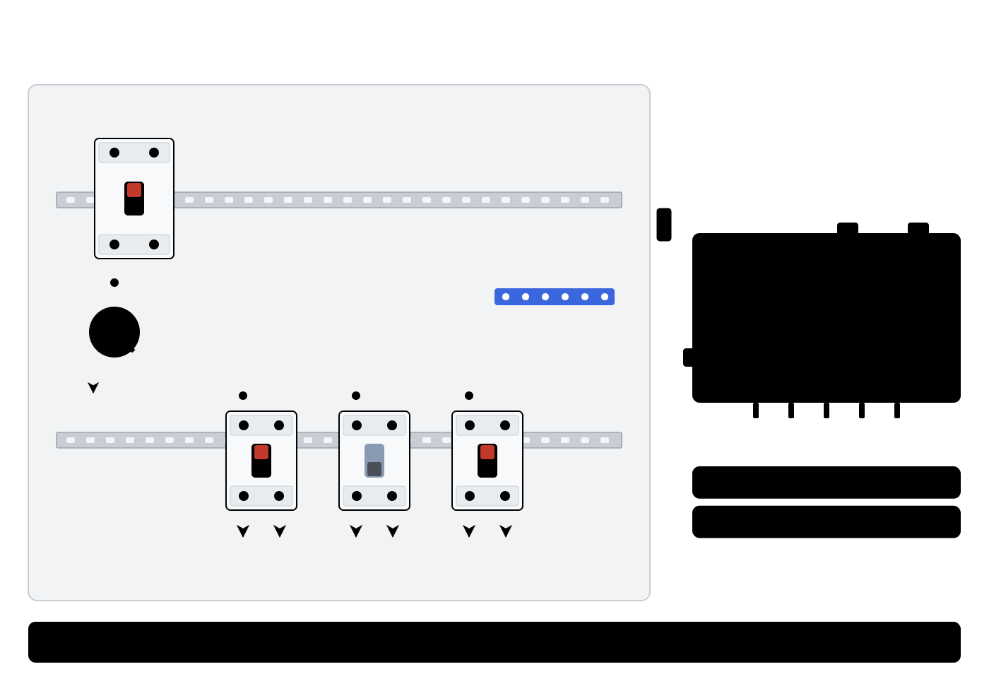
Voltage sensor (UI* variants)
The PCB exposes L (line / phase) and N (neutral) terminals. Polarity matters for the sign of active power:
- Correct wiring (L → L, N → N):
P > 0means consumption (current flowing into the load from the grid),P < 0means export to the grid (generation). - Swapped wiring (L and N exchanged): the sign of P is inverted — consumption is reported as negative power.
Wire and fuse. A thick wire is not required for the voltage connection: AWG26–22 is enough, because the voltage sensor draws very little current. A fuse in the L line is mandatory, rated up to 0.1 A.
Correct polarity is critical for:
- Accurate BASIC-tier accounting (BASIC counts only
max(P, 0); swapped polarity zeros out the energy total). - Correct separation of consumption and generation on the STD line.
Quick check: with a purely resistive load (electric kettle, heater, incandescent bulb),
P > 0andPF ≈ 1.0. If P is negative while the load is consuming, swap L and N on the PCB.
Current sensor — SCT-013 (for SKUs with external CT)
SCT-013 clamps connect to the module through a 3.5 mm jack. The connector is keyed for correct polarity out of the box; no wiring decisions are needed. Characteristics of each SCT-013 rating (floors, class, tolerance, clipping): see the SCT-013 table.
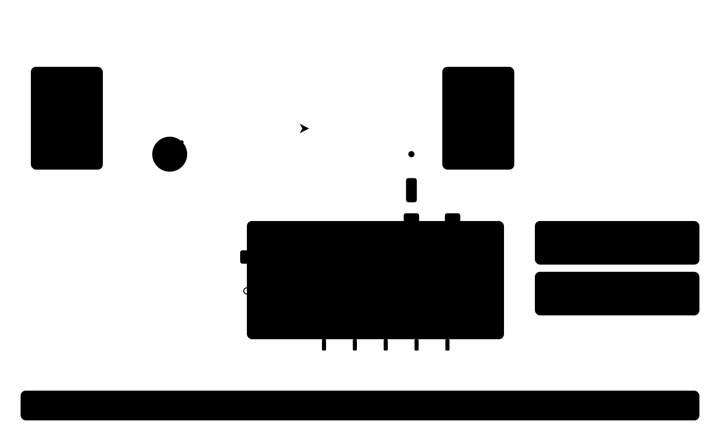 The clamp body bears an arrow indicating the direction of energy flow for the "normal" orientation:

Rules:
- Clamp the sensor around the line (L) wire going to the consumer.
- The arrow on the clamp must point in the direction of current toward the load (from breaker panel to load).
- The clamp must close completely — no gap between the two halves of the magnetic core. A gap > 0.1 mm sharply increases magnetic reluctance and degrades accuracy.
⚠️ Warning: do not pass both L and N through the same clamp. Their magnetic fluxes are equal and opposite, so they cancel — the sensor reads near zero current even under real load.
Channel markings on the PCB
Each jack on the PCB is labeled with the channel name (I0, I1, I2, …) and a color marker. SCT-013 cables are electrically symmetric — orientation is established by the arrow on the clamp and its placement on the wire, not by which end of the cable goes into the jack.
Polarity and the sign of P
- Arrow in the correct direction + correct L/N polarity →
P > 0for consumption,P < 0for export. - Clamp installed reversed (arrow against current direction) → the sign of P is inverted.
Current clamps — CT series
Each channel of a CT-series module has its own clamp on a 1 m cable. The cable arrives connected to the module and is marked with the channel number; connect it to the plug-in connector of that channel. Keep each clamp on its own channel, also when you rewire the panel later: a clamp on another channel gives wrong readings, and the module does not report it.
- Do not move a clamp to another channel and do not connect another clamp: the calibration belongs to the pair.
- Fit the clamp on the L conductor with the arrow pointing toward the load (the consumer); the conductor must go through the window and the clamp must close fully.
- Window size follows the rating: 6 mm for 1–10 A, 10 mm for 20–50 A, 16 mm for 100 A. The conductor with its insulation must fit the window.
- Power and bus, pull-ups, bus speed, voltage wire and fuse: as for every BASIC module (see the sections above). The voltage input is the same as on the SCT-UI modules: wire AWG26–22, a fuse in the L line up to 0.1 A.
DATA_READY (DRDY)
Optional pin for optimized polling. If your application is happy polling on its own fixed interval (100 ms or slower), you can leave DRDY disconnected.
Electrical parameters
- Output type: open-drain (no active pull-up to VCC)
- Idle level: HIGH (requires a pull-up on the master side — either an internal MCU pull-up or an external resistor; recommended 10 kΩ to 3.3 V)
- Ready pulse: LOW for ~10 µs, after RT registers (
0x86..0xCF) have been refreshed - Pulse frequency: ~10 Hz (one pulse per ~100 ms RT window; ~5 Hz on images before v1.2)
Semantics
The falling edge of DRDY guarantees that all RT registers are coherent and freshly published (the firmware updates them atomically inside an ISR before lowering the pin). The master can read 0x86..0xCD immediately on the falling edge with no risk of a split sample.
Master-side usage
- EXTI / GPIO interrupt on the falling edge — wakes the master and triggers a read.
- Use any input-capable GPIO — the pin numbers in the examples (e.g. GPIO 15) are illustrative, not a requirement.
- Pull-up 10 kΩ to 3.3 V on the master side.
- Multiple module DRDYs can be combined into a wired-OR (see realtime-polling.md → Multi-module DRDY).
Applicability
- DRDY fires only on RT updates (every measurement window, ~100 ms from v1.2).
- DRDY does not fire on period snapshots (period snapshots are updated by the snapshot command which the master triggers — so the master already knows when to read).
- For slow-polling masters (every 1 s or 60 s), DRDY can be ignored.
In the client libraries — the same task without register access:
Library Call What it does Arduino RbAmp::setDrdyPin(pin)/RbAmp::waitDataReady(timeout_ms, ev)attach the DRDY pin; wait for the next published window ESP-IDF rbamp_set_drdy_gpio()/rbamp_wait_data_ready()attach the DRDY pin; wait for the next published window Python — the library does not use the DRDY pin ESPHome drdy_pin:optional DRDY input; only logged, not used as a read trigger
Reference wiring example (ESP32, single module)
Other module variants
Other module variants use the same LV-side pinout (VCC / GND / SDA / SCL / DRDY); only the mains side differs.
Next
- initialization.md — first connection, smoke test, address change
- troubleshooting.md → CT clamp & polarity — what to do if the sign of P is wrong or I_rms is unstable