04 · Wiring
This chapter describes the physical wiring of the rbAmp module to ESP32-family boards: LV-side pinout, power requirements, I²C voltage-level compatibility, bus length, and the standard default pins for the 7 supported ESP32 chips (esp32, esp32s2, esp32s3, esp32c2, esp32c3, esp32c6, esp32h2).
The module's mains side is galvanically isolated from the LV side. The
LV side (power + I²C + optional DRDY) is described first; the mains
and CT connection is in Mains and CT connection
below.
LV-side pinout
 The module runs on 3.3 V I²C logic and is 5 V-tolerant on the
signal lines. All LV pins are fully galvanically isolated from mains.
| Pin | Signal | Purpose |
|---|---|---|
VCC |
+5 V (4.5..5.5 V) | Module power; minimum 4.5 V for correct operation |
GND |
Ground | Shared with the master — mandatory |
SDA |
I²C SDA | I²C data |
SCL |
I²C SCL | I²C clock |
DRDY |
Data-ready (optional) | Open-drain, LOW pulse ~10 µs every ~100 ms |
Power
VCC parameters
- Nominal voltage: 5 V DC
- Allowable range: 4.5..5.5 V
- Current draw: ~15 mA typical, ~25 mA peak during flash writes
- Ripple: < 50 mV peak-to-peak (for measurement accuracy)
The module carries an on-board regulator, RC filter, ceramic capacitors
and a ferrite bead — no additional filtering is required from the user.
The module can be powered from the +5V or +5V0 rail of any DevKitC
board (USB-5V powered).
I²C voltage-level compatibility
SDA/SCLoperate at 3.3 V logic (built-in pull-ups pull the lines to 3.3 V).- The lines are 5 V-tolerant, but the ESP32 family is already at 3.3 V anyway — no level shifters are required.
- The ESP-IDF
i2c_masterdriver uses open-drain outputs on the GPIO — compatible with the module's built-in pull-ups.
Power-up behavior
- Cold start: ~250 ms to the first valid result.
- After a reset (software or brown-out): ~250 ms to recover.
- Until the first valid result the registers read as
0, with theDATA_VALIDflag = 0.
The component waits for the module to become ready inside
rbamp_begin(dev) itself — user code simply calls rbamp_begin() and
continues.
Isolation
Inside the module there is a galvanic isolation barrier between the mains side (CT clamp, voltage divider) and the LV side (I²C). Consequences:
- The module's
GNDis not connected to mains line or neutral. - The LV side is isolated from the mains side by the barrier, so the LV pins connect to the ESP32 without a mains reference. This does not replace the mains-wiring precautions in the next section.
⚠ Do not open the module enclosure — this voids the factory calibration.
Mains and CT connection
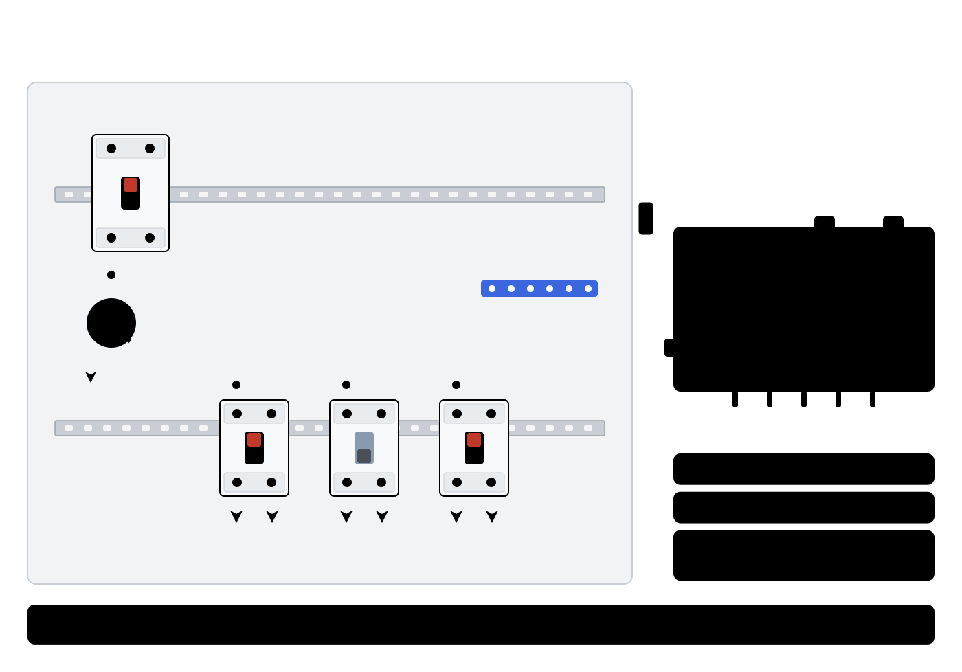
⚠ Mains voltage can kill. Disconnect and lock out the circuit before connecting the L/N terminals or fitting the clamp; have a qualified person do mains wiring and any work inside a panel. Clamp ONE conductor only (L) — never the whole cable. Fuse the L tap per local rules (mandatory, up to 0.1 A; AWG26–22 wire is enough — the voltage sensor draws very little current).
- Voltage (UI variants only): the module measures voltage from the L/N
connection on its mains side: the PCB exposes
L(line) andN(neutral) terminals, and polarity matters for the sign of power. I-variants (I1/I2/I3) have no voltage input. - Current: the SCT-013 clamp plugs into the module's 3.5 mm CT jack (keyed for correct polarity; each jack
on the PCB is labelled with its channel,
I0,I1, …) and closes around the line conductor (L). The arrow on the clamp body points in the direction of current toward the load. A reversed clamp gives a negativePon a consuming load. - Clamp the line conductor, not neutral and not both conductors together.
- Do not open the module enclosure — this voids the factory calibration. The pull-up bridges mentioned below are on the board's bottom side; follow the module's instructions for reaching them.
Built-in pull-up resistors — on-board
Important: every rbAmp module has built-in 4.7 kΩ pull-up resistors on SDA and SCL to 3.3 V. For a single module on the bus no external pull-ups are required — connect the ESP32 directly.
The ESP-IDF i2c_master_bus_config_t also lets you enable the
internal GPIO pull-ups via flags.enable_internal_pullup = true.
They are weak (~50 kΩ on the ESP32) and work in parallel with the module's
external 4.7 kΩ — the combination gives an effective ~4.4 kΩ, which is
acceptable. For production deployments, prefer relying on the module's
external 4.7 kΩ; the internal GPIO pull-ups are optional with the module's
own pull-ups and are mainly for bench tests without a module on hand (for
example, when you are just checking a bus scan).
When to disable the built-in pull-ups
If there are several rbAmp modules on the bus (or other I²C devices with their own pull-ups), wiring them in parallel yields an effective resistance that is too low, which:
- Increases bus current draw
- May exceed the maximum sink current of the I²C master output stage
- Adds capacitive load on a long bus while doing little to improve noise immunity
Solution: on the bottom side of each module's board, next to the pull-up
resistors, there are jumper bridges (silkscreen Pull-Up). Cut them
with a sharp blade:
- Leave the pull-ups enabled on only one module (or move them to a single point near the ESP32).
- Cut the bridges on the remaining modules.
Rule of thumb
 | rbAmp modules on the bus | Pull-ups |
|:---:|---|
| 1 | Leave as-is (the built-in 4.7 kΩ works) |
| 2 | Leave on one, cut on the other |
| 3 | Cut on all modules, fit one external 2.7…3.3 kΩ pair near the ESP32 |
| 4…6 | Cut on all modules, one external 2.2…2.7 kΩ pair near the ESP32 |
| 7…16 | Cut on all modules, one external 1.5…2.2 kΩ pair near the ESP32; check the bus capacitance (≤ 400 pF), lower the bus speed if needed |
The external values are recommended values (calculated from the I²C specification: sink current ≤ 3 mA at 3.3 V, bus capacitance ≤ 400 pF). Connect the external pull-ups to 3.3 V (the logic level of the bus), not to the 5 V VCC supply.
If in doubt: measure the resistance between SDA and the 3V3 line with all devices unpowered. It should be in the 1.5..4.7 kΩ range. Lower — too many active pull-ups in parallel.
I²C bus parameters
- Default address:
0x50(7-bit) - Address range:
0x08..0x77(reassignable at the factory) - Recommended speed on ESP32: 50 kHz (see the section on the retry+sanity discipline below)
- Pointer auto-increment: on reads only. A burst-read
<addr> + N bytesreturns N consecutive bytes starting ataddr(auto-increment). Writes are NOT auto-incremented: a burst-write<addr> + N byteslands only the first byte, the rest are dropped. Multi-byte registers are written byte by byte — a separate single-byte transaction per address. For details see 09 · API Reference, the “Multi-byte writes” section.
Bus length
I²C is a short bus (~15 cm by default). Many users connect modules with low-quality jumper wires, which pick up a lot of noise and lose many transfers — hence the short limit. Recommended topologies for rbAmp:
| Cable | Max length | Speed |
|---|---|---|
| Standard JST / flat 4-conductor | up to 0.15 m | 100 kHz |
| Twisted-pair UTP (cat-5/5e/6) — SDA+GND and SCL+GND in separate pairs | up to 1 m | 100 kHz |
| Twisted pair + I²C buffer (PCA9515 / TCA9617) | up to 3 m | 100 kHz |
| Differential bus (PCA9615 / LTC4332) | up to 100 m | 100 kHz |
The lengths above were verified at 100 kHz. The component's default bus speed is 50 kHz (see "ESP32 baseline NACK pattern" below), which is more tolerant of longer cables; keep 50 kHz and do not exceed these lengths.
For lengths beyond 0.15 m a twisted pair is mandatory: SDA and SCL must be in different pairs, each with its own ground. SDA and SCL in the same pair create cross capacitive coupling that distorts the edges.
⚠ Inside an electrical cabinet, shield the I2C cable. Strong magnetic fields near mains conductors, contactors and transformers induce noise in an unshielded cable. Keep the cable as short as possible and away from the mains wiring.
Multi-module bus — the primary topology
The library's canonical use case is several rbAmp modules on a single I²C bus, managed by one ESP32 via a fleet handle. All the rules and optimizations below are designed precisely for this topology; a single module is a special case (the same handle, but the fleet calls degenerate into trivial ones).

Typical deployments
| Scenario | Configuration | Module count |
|---|---|---|
| 80% canonical: home main + submeters | 1× UI1 (main, mains-energy) + 3-6× UI1 (loads; power and Wh need a UI variant) | 4-7 |
| Subpanel with current breakdown | 1× UI1 (main) + 1-2× I2/I3 (per-circuit current) | 3-5 |
| Industrial sub-metering | 1× UI1 (main) + N× I2/I3 (per machine, current breakdown) | up to ~16 |
Electrical constraints
- Module count: up to ~16 (total bus capacitance ≤ 400 pF at 100 kHz).
- Addresses: each module has its own 7-bit address (range
0x08..0x77). All modules ship from the factory on0x50— re-address them one at a time before wiring them in parallel (see below on two-phase commit and provisioning viarbamp_provision()). - Pull-ups (important for a fleet bus): the ESP32-internal pull-ups (~45 kΩ) are too weak for a multi-module bus with long traces and noise. For reliable operation you need external pull-ups (2.7…3.3 kΩ for 3 modules, lower for larger buses — see the table above) to 3.3 V on SCL/SDA at a single point on the bus + the built-in pull-ups cut on all modules but one (or cut on all and keep only the external ones). This is part of the three-layer mitigation against bus-hang on a marginal bus — see 10 · Troubleshooting.
Addressing — provisioning and field-swap
The default factory address is 0x50. Each new or replacement module goes
through provisioning (once): re-addressing from 0x50 to a working
address + optional saving of the configuration (CT model, group_id, label)
to flash.
In code this is a single call — rbamp_provision(bus, desired_addr, save_config, &dev). It verifies that there is really only one virgin module on 0x50 on the bus, re-addresses it via a two-phase commit (see below), optionally saves the user config, and returns a ready handle.
⚠ Provisioning discipline (MUST): there must be exactly one virgin module (on
0x50) on the bus at the momentrbamp_provision()is called. If two modules at the same address respond on I²C simultaneously — a collision on the data phase, behavior is undefined, and there is no way to distinguish them (open-drain wired-AND). Recovery path: power-cycle, switch physically to a single-module bring-up, provision them one at a time, then connect the rest. See 10 · Troubleshooting, the “Provisioning fail / address conflict” section.If you do not have a fleet handle and you re-address manually via
rbamp_prepare_address_change()+rbamp_commit_address_change()(the low-level form) — the discipline is exactly the same: one virgin at a time.
Two-phase commit for an address change
The firmware supports an address change in production mode via a two-phase sequence:
1. write candidate_addr → REG_I2C_ADDRESS (0x30, in RAM)
2. write 0xA5 → REG_ADDR_COMMIT_MAGIC (0x31, armed)
3. issue CMD_COMMIT_ADDR (opcode 0x30 in REG_COMMAND)
4. issue CMD_RESET (0x01)
5. wait ~300 ms; the new address is active
The component wraps this in rbamp_prepare_address_change() / rbamp_commit_address_change() — see 09 · API Reference. Persistence is confirmed only after a reset (see the “Production vs Factory mode” callout in 03_sensor_selection.md).
Bus energy budget — how many modules your polling rate can sustain
On a 50 kHz bus a single register-read transaction ≈ 200-400 µs (depends on the MCU driver). A full RT block of one channel (U + I + P + PF) = 4 floats = 16 bytes + 4 address phases ≈ 5-8 ms per channel.
| Configuration | Bus per cycle | At 50 kHz | Max polling rate |
|---|---|---|---|
| 1× UI1, RT block | ~5 ms | < 5 ms | 100+ Hz (but the module updates at 10 Hz) |
| 1× I3, RT block + period | ~25 ms | ~25 ms | up to 10 Hz |
| 5× UI1, RT block | ~25 ms | ~25 ms | up to 10 Hz |
| 16× I3, RT + period | ~400 ms | 400 ms > 100 ms | cannot keep up with the module (10 Hz); ~2 Hz at best |
The numbers above are estimates and depend on the host MCU and driver.
Rule: at 50 kHz the comfortable limits are 8-10× I3 or 15-16× UI1 at 5 Hz polling (every second module window), and roughly half of that at the full 10 Hz. Beyond that:
- Lower the polling rate (1 Hz = 10× headroom).
- Move to 100 kHz with retry (expect frequent NACKs and rely on retry).
- Use the DRDY pin for async — do not poll modules that are not ready yet.
Period sync — synchronizing periods for tight synchronization
For tariff metering all modules must take their snapshot over the same time interval. Two strategies:

Strategy 1 — sequential snapshot + shared settle (works on any firmware):
/* Phase 1: sequential snapshot */
for (int i = 0; i < n; i++) {
    rbamp_latch_period(devs[i]);
}
/* Phase 2: shared settle (≥ 50 ms for the snapshot + ~1 commit cycle for witness) */
vTaskDelay(pdMS_TO_TICKS(50));
/* Phase 3: read snapshots with skip_latch=true */
rbamp_period_snapshot_t snaps[n];
for (int i = 0; i < n; i++) {
    rbamp_read_period_snapshot(devs[i], &snaps[i], 0, /*skip_latch=*/true);
}
Skew between modules: 16 modules × ~1 ms/snapshot = ~16 ms relative to a 60-second period → 0.027%. Negligible.
Strategy 2 — General-Call broadcast snapshot (requires enabling):
All modules receive the snapshot in a single I²C frame on addr 0x00:
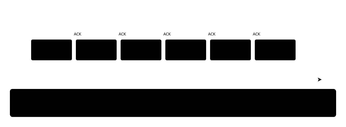
addr=0x00 | A5 27 <group> <tick_lo> <tick_hi> (5 bytes)Skew = 0 (atomic). Pre-config:
- On each module enable
REG_FLEET_CONFIG.bit0 = 1viaCMD_SAVE_USER_CONFIG. CMD_RESET— GC reception is activated at boot.- After the reset the master sends the 5-byte frame.
- Witness: for each expected module read
REG_V03_PERIOD_VALID (0x07).!=1→ fall back to strategy 1.
When to use which: - < 8 modules: strategy 1 (simpler, no enabling required). - ≥ 8 modules or tight synchronization: strategy 2.
GC group filtering — a multi-tenant bus
REG_GROUP_ID (0x28) lets you have several GC domains on a single bus:
group = 0x00→ all-call (all modules with GC enabled take the snapshot).group = N→ only modules withREG_GROUP_ID = Ntake the snapshot.
Example: a bus with 10 modules, where you need to snapshot 5 for tariff A and 5 for tariff B independently:
write REG_GROUP_ID = 1 on the 5 tariff-A modules
write REG_GROUP_ID = 2 on the 5 tariff-B modules
GC frame [A5 27 01 tl th] → only tariff A takes a snapshot
GC frame [A5 27 02 tl th] → only tariff B takes a snapshot
GC frame [A5 27 00 tl th] → all 10 take a snapshot (all-call)
Failure modes on a multi-module bus
| Symptom | Cause | What to do |
|---|---|---|
i2c bus scan shows several modules at the same address after a field add |
The new module on 0x50 conflicts with an already-addressed one |
Re-flash the new module's address separately before adding it to the bus |
| One module starts NACK'ing more often than the others | Cable fault / VCC drop on that module | Check VCC under load + logic levels |
| One module's Wh consistently diverges | The module's own timer differs from the master clock | Integrate energy against the master clock (master_dt_ms) |
| After a GC frame one module does not take the snapshot | FLEET_CONFIG.bit0 = 0 or group mismatch |
Check REG_FLEET_CONFIG and REG_GROUP_ID |
Bus design notes
- Clock stretching: the current firmware minimizes stretch (the
__disable_irqwindow in LatchPeriod is short, ~µs). The snapshot itself does not pull SCL significantly. For the Raspberry Pi BCM283x (a known clock-stretching hw bug): apply the standard caution — 50 kHz + retry are already recommended. - Bus length with >4 modules: even on a twisted pair the effective capacitance grows linearly with the count. Consider an I²C buffer (PCA9515) at ≥ 8 modules + a length > 1 m.
Detailed multi-module scenarios are in 06 · Examples, the “Sub-metering shared bus” and “GC broadcast snapshot” scenarios.
Pinout on the ESP32 family
The 7 chips listed at the top of this chapter are supported (per idf_component.yml). Below are the
recommended default pins for I²C; for production deployments, choose the
GPIO based on your board's specific layout.
ESP32 (original / DevKitC / WROOM)
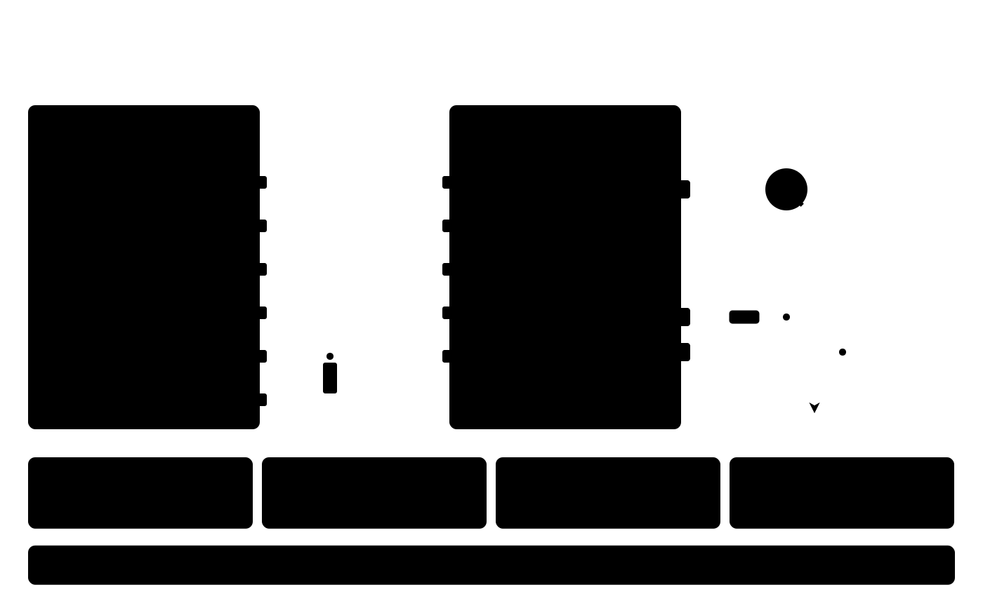
const i2c_master_bus_config_t bus_cfg = {
    .i2c_port  = I2C_NUM_0,
    .sda_io_num = GPIO_NUM_21,
    .scl_io_num = GPIO_NUM_22,
    .clk_source = I2C_CLK_SRC_DEFAULT,
    .glitch_ignore_cnt = 7,
    .flags.enable_internal_pullup = true,
};| Pin | GPIO |
|---|---|
| SDA | GPIO21 |
| SCL | GPIO22 |
| DRDY | any free GPIO that is not a strapping pin (on the classic ESP32 avoid GPIO0/2/12/15) |
ESP32-S2
The same default GPIO21/22 as the original ESP32. The S2 has no Bluetooth — an extra ~30 kB of heap is available for TLS scenarios.
ESP32-S3
The S3 has no hardware-fixed I²C defaults — any GPIO via the matrix. On
most WROOM-S3 dev boards GPIO8/GPIO9 are a comfortable choice (check your
board's schematic: on the N16R8 these pins may be taken by QSPI flash;
USB-JTAG occupies GPIO19/20). Adjust the sda_io_num / scl_io_num
fields in i2c_master_bus_config_t:
.sda_io_num = GPIO_NUM_8,
.scl_io_num = GPIO_NUM_9,
The S3 has USB-OTG — it can be used for debugging without an external USB-UART chip.
ESP32-C2 / C3 / C6 / H2
RISC-V single-core chips (the C3 and C6 are single-core; the H2 is single-core with BLE+802.15.4; the C2 is single-core with limited RAM). The I²C pins are not hardware-fixed — here is an example for the ESP32-C3 (on the C3-SuperMini GPIO5/GPIO6 are comfortable; on the C3-DevKitM-1 USB-JTAG occupies GPIO18/19, and GPIO8/9 are strapping):
const i2c_master_bus_config_t bus_cfg = {
    .i2c_port  = I2C_NUM_0,
    .sda_io_num = GPIO_NUM_5,
    .scl_io_num = GPIO_NUM_6,
    .clk_source = I2C_CLK_SRC_DEFAULT,
    .glitch_ignore_cnt = 7,
    .flags.enable_internal_pullup = true,
};
For the other chips — check the target-specific ESP-IDF documentation
(docs.espressif.com → ESP-IDF v5.2+ → your chip → API reference →
peripherals → I2C).
ESP32-P4 — not a supported target
The ESP32-P4 is not in the supported target list: P4 support needs
ESP-IDF v5.3+, while the component's minimum is v5.2 (a v5.2 build for
esp32p4 would fail with “target esp32p4 not in idf”).
ESP32 baseline NACK pattern — 50 kHz bus speed
With the ESP-IDF v5 i2c_master driver, rbAmp exhibits frequent NACKs
at 100 kHz, far fewer at 50 kHz (a characteristic of the driver
on the ESP32 side, not the slave). The component covers this in two layers:
- A default bus speed of 50 kHz via the Kconfig
CONFIG_RBAMP_DEFAULT_I2C_FREQ_HZ=50000. The component requests this frequency when adding its device handle to the bus you create. - Per-byte retry —
CONFIG_RBAMP_NACK_RETRY_ATTEMPTS=3× 5 ms gap. At 50 kHz the residual error rate is < 0.8%.
Override via idf.py menuconfig if needed:
CONFIG_RBAMP_DEFAULT_I2C_FREQ_HZ=50000
CONFIG_RBAMP_NACK_RETRY_ATTEMPTS=5     # for dense workloads
CONFIG_RBAMP_NACK_RETRY_GAP_MS=5
CONFIG_RBAMP_I2C_TIMEOUT_MS=200
For more on diagnosing bus-level problems — see 10 · Troubleshooting.
DATA_READY (DRDY)
An optional pin for polling optimization. If the application polls the
module no more often than once every 100 ms — DRDY can be left
unconnected.
Electrical parameters
- Output type: open-drain (no active pull-up to VCC)
- Idle level: HIGH (requires a pull-up on the master side — an
internal
gpio_pullup_en()or an external resistor; 10 kΩ to 3.3 V is recommended) - Ready pulse: LOW for ~10 µs after the RT registers have been updated with fresh data
- Pulse rate: ~10 Hz (one pulse per ~100 ms RT window)
Semantics
A falling edge on DRDY guarantees that all RT registers are
synchronized and published (the firmware updates them atomically in the
ISR before lowering the pin). After the falling edge the master can read
the RT block with no risk of getting a split sample.
Interrupt pattern — FreeRTOS semaphore
ESP-IDF offers a clean model: an ISR in IRAM raises a binary semaphore, a separate FreeRTOS task waits on the semaphore and reads RT.
#include "freertos/FreeRTOS.h"
#include "freertos/task.h"
#include "freertos/semphr.h"
#include "driver/gpio.h"
#define DRDY_GPIO GPIO_NUM_4   /* a free GPIO; do not use
                                 * GPIO0/2/12/15 — strapping pins
                                 * (ESP32 classic), they can disrupt boot
                                 * if the open-drain DRDY goes LOW
                                 * during reset */
static SemaphoreHandle_t drdy_sem;
static void IRAM_ATTR drdy_isr_handler(void *arg) {
    BaseType_t hi_task_woken = pdFALSE;
    xSemaphoreGiveFromISR(drdy_sem, &hi_task_woken);
    if (hi_task_woken) portYIELD_FROM_ISR();
}
void bidir_task(void *arg) {
    rbamp_handle_t dev = arg;
    while (1) {
        if (xSemaphoreTake(drdy_sem, portMAX_DELAY) == pdTRUE) {
            float p;
            if (rbamp_read_power(dev, 0, &p) == ESP_OK) {
                /* integrate + publish */
            }
        }
    }
}
void app_main(void) {
    /* ...rbamp_new + rbamp_begin... */
    drdy_sem = xSemaphoreCreateBinary();
    /* The ISR service is installed ONCE for the whole project — if another
     * component (LCD, encoder, anything) has already installed it,
     * gpio_install_isr_service() returns ESP_ERR_INVALID_STATE.
     * This is normal, do not fail on it. ESP_INTR_FLAG_IRAM keeps the
     * ISR dispatcher in IRAM — important for the single-core C3/C6/H2/S2,
     * where non-IRAM code is unavailable while the flash cache is disabled. */
    esp_err_t err = gpio_install_isr_service(ESP_INTR_FLAG_IRAM);
    if (err != ESP_OK && err != ESP_ERR_INVALID_STATE) {
        ESP_ERROR_CHECK(err);
    }
    gpio_config_t io_cfg = {
        .pin_bit_mask = 1ULL << DRDY_GPIO,
        .mode         = GPIO_MODE_INPUT,
        .pull_up_en   = GPIO_PULLUP_ENABLE,
        .pull_down_en = GPIO_PULLDOWN_DISABLE,
        .intr_type    = GPIO_INTR_NEGEDGE,
    };
    gpio_config(&io_cfg);
    gpio_isr_handler_add(DRDY_GPIO, drdy_isr_handler, NULL);
    /* Priority 6 — above idle (0), below WiFi (23) and the standard
     * MQTT (5+). 4096 bytes of stack are enough for rbamp_read_* +
     * ESP_LOG; if you add an MQTT publish right in this task —
     * raise it to 6144. On dual-core ESP32/S3, for a clean
     * separation from the WiFi task (usually core 0), you can pin
     * this task to core 1: xTaskCreatePinnedToCore(..., 1).
     * On the single-core C3/C6/H2/S2 — keep xTaskCreate. */
    xTaskCreate(bidir_task, "bidir", 4096, dev, 6, NULL);
}
DRDY is optional — polling at any rate ≤ 10 Hz works without it too.
The component does not depend on DRDY in any of its paths.
Links
- 05 · Quickstart — your first working project
- 06 · Examples — working scenarios (including the multi-module bus)
- 09 · API Reference — the “Kconfig symbols” section for detailed configuration of I²C parameters
- 10 · Troubleshooting — bus-level debug, NACK pattern, retry+sanity discipline
Source & issues: rb-amp/rbamp-esp-idf · this page in the repo: docs/04_hardware.md (v1.7.3)